Semiconductor Thin Films
Thin film materials for semiconductor manufacturing
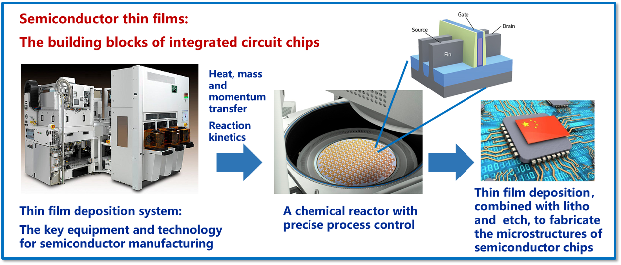
Thin film deposition is among the key processes of semiconductor manufacturing. By designing and building thin film deposition tools such as atomic layer deposition (ALD) and plasma enhanced chemical vapor deposition (PECVD), we study the deposition mechanisms and material properties of metallic, dielectric, and semiconductive thin films, which could be used as high-k dielectric layers, etching hardmasks, EUV dry resists and etc in semiconductor manufacturing processes.
1. Atomic layer deposition
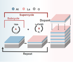
Miniaturization in the semiconductor industry has led to the requirement for atomic level control of thin film deposition. Miniaturization has produced very high aspect structures that need to be coated conformally. No other thin film technique can approach the conformality achieved by ALD on high aspect structures. ALD is able to meet the needs for atomic layer control and conformal deposition using sequential, self-limiting surface reactions.
Current projects include:
●Deposition of metal and metal oxide films
●Corrosion-resistant multilayer ceramic film deposition
2. Molecular Layer Deposition for Next-Generation Hybrid Photoresists
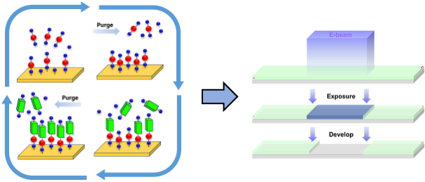
Driven by the urgent demand of advanced micro/nanofabrication for higher resolution and lower defectivity, and the difficulty of simultaneously achieving high sensitivity, low line-edge roughness, and strong etch resistance for conventional photoresists under advanced lithography (e.g., EUV), it is of great significance to develop next-generation resists and fabrication strategies with precisely controllable structures. We are exploring molecular layer deposition (MLD) to construct inorganic–organic hybrid photoresists, enabling programmable control over film thickness, composition, and ligand architecture via atomic-/molecular-scale layer-by-layer growth. This approach effectively mitigates chemical stochasticity and improves resist performance.
Current projects include:
●MLD of high-sensitivity hybrid resists with strong etch resistance
●Mechanistic studies of exposure-driven reactions to minimize LER/LWR
3. Area-selective atomic layer deposition
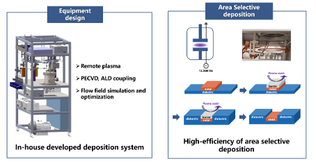
Area-selective atomic layer deposition (AS-ALD) is recognized as a novel patterning approach in nanostructure fabrication, serving as a promising alternative to conventional top-down lithography steps. This bottom-up thin-film deposition technique significantly simplifies the manufacturing of nanostructures while maintaining high precision at minimal feature sizes. Our research focuses on the design of film deposition equipment architectures to integrate multiple deposition steps.
By precisely modulating the surface chemistry of different substrates, we achieve controlled adsorption and nucleation of precursors on specific surfaces. This endeavor aims to explore new possibilities for next-generation nanomanufacturing technologies.
Current projects include:
●Dielectric on dielectric (DoD) AS-ALD
●Metal on metal (MoM) AS-ALD
4. Atomic layer etching

Atomic Layer Etching (ALE) is a cyclic, self-limiting etching technology that enables atomic-scale thickness control, exceptional selectivity, and ultra-low-damage processing. ALE provides ultra-smooth surfaces and highly anisotropic profiles, making it essential for advanced semiconductor fabrication and high-aspect-ratio 3D structures. Our research focuses on etching mechanisms and self-limiting surface chemistry, plasma-enhanced and low-temperature ALE processes, selective etching strategies and mask/stop-layer engineering, as well as wafer-scale uniformity and profile control. By bridging atomic-level surface science with scalable process engineering, we aim to develop next-generation ALE technologies that enable high-performance logic devices, 3D NAND, MEMS, and quantum architectures.
Current projects include:
●Thermal ALE for Next-Generation Metal Interconnects
●Plasma-Enhanced ALE of High-k Dielectric Layers